
Introduction
Many industries require thin layers of materials to be adhered to surfaces to build functional devices, prostetics, and sensors. In Augest of 2024 I was approached by a design called HackerFab at the University of Waterloo to aid in the creation of a DC sputter chamber. The intent of the sputter deposition chamber by HackerFab is for open-source semiconductor fabrication. During the development of the preliminary V0 and of the first complete version, V1, I was the mechanical design lead. As of May 2025 I have taken up an advisor role instead of a lead role on this project to focus on other projects within HackerFab.
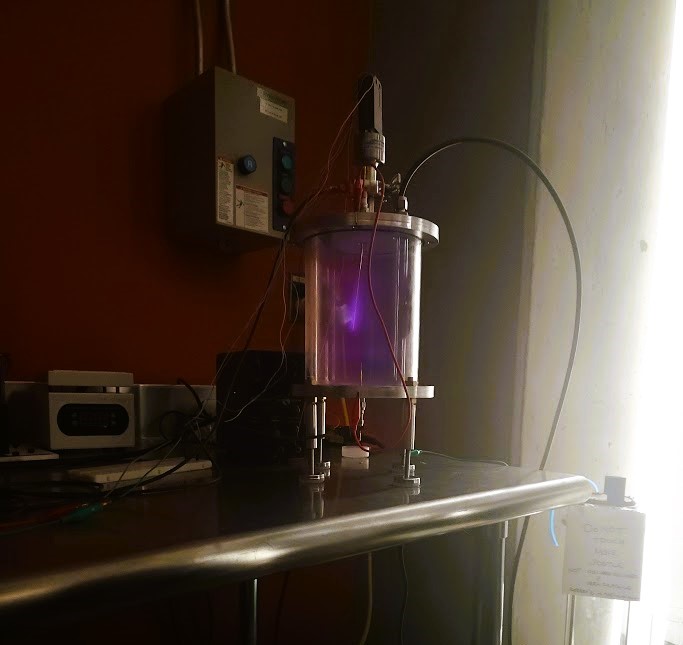
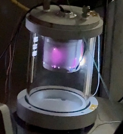
This project was an enlightening experience for designing vacuum chambers, safely integrating high voltage componants, and creating plasmas for practical applications. In addition to the experiences building this device I also had the opportunity to “lecture” newer members of HackerFab about the fundamentals of CAD design on OnShape, and the physics and chemistry that act as the background for the sputter chamber’s functionality.
Sputter V0
Augest 2025 - December 2025
Sputter V0 was intended to be a small start for the team gaining our bearings to make a fully fledge sputter chamber. The entire chamber was designed in roughly 3 months and machined and assembled in roughly a month for approximatly $300 CAD with help from the machinists from Ascension Automation in Cambridge, ON.
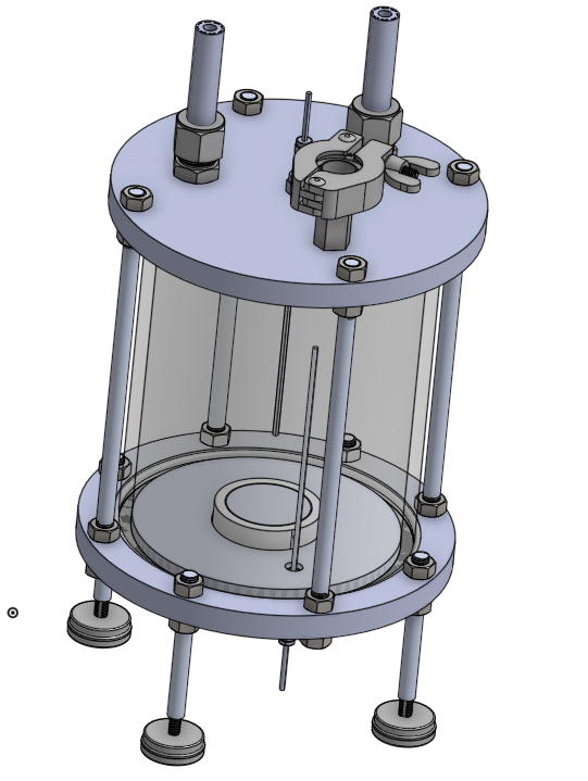
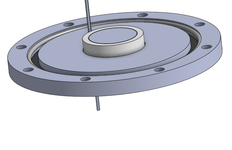
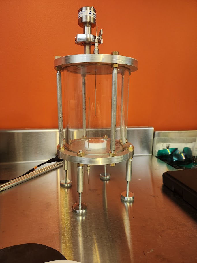
A generic form factor between the subsequent iterations of the sputter deposition chamber originated from V0. This form factor is characterized by a 5.5” borosilicate tube to see the plasma in the chamber and two plates sealed with radial sealing O-rings.
Sputter V1
January 2025 - March 2025
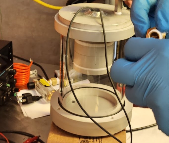
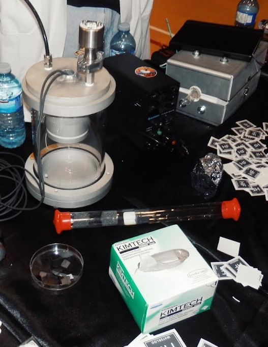
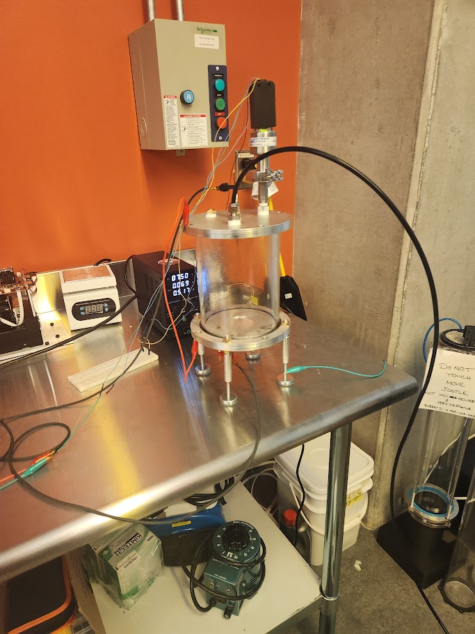
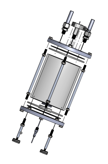
Sputter V1 is the first attempt at a fully fledged sputter deposition chamber. The changes from sputter V0 to V1 include some small ease of use changes and the addition of a sputter head. This design costed roughly $1100 CAD and was machined by PCBWay and JLCPCB.
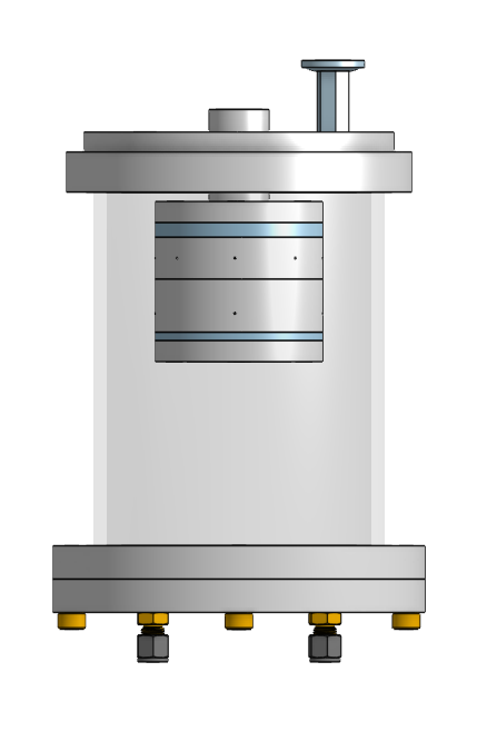
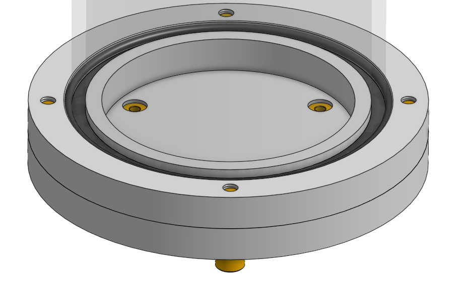
The quality of life changes stem from the major issue with V0 being the lack of ease of access of the silicon substrait inside the chamber. The raidal seals offer too much friction to allow the inside of the chamber to be easily accessed. This was resolved by having radial sealed O-rings seal the borosilicate tube to a lid ring, while the chamber lid is sealed with a face sealed O-ring.
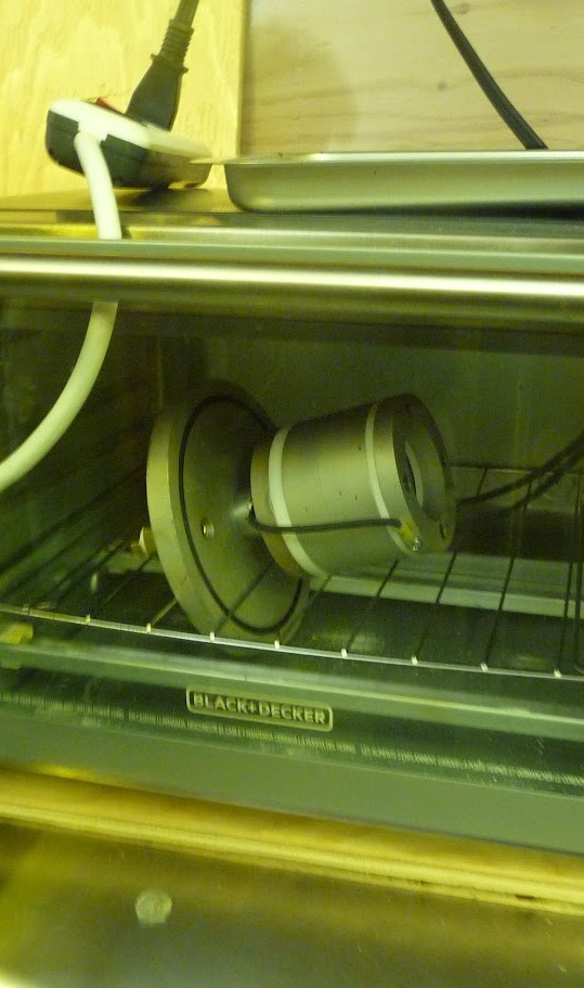
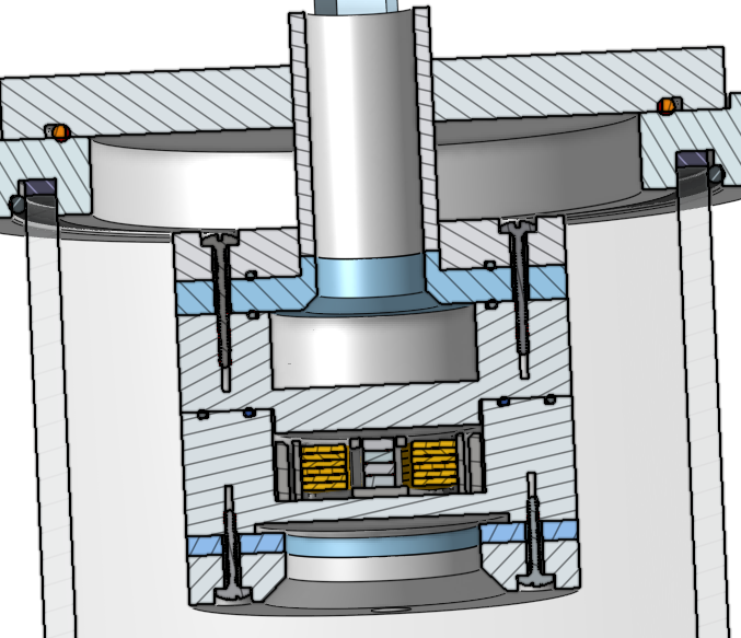
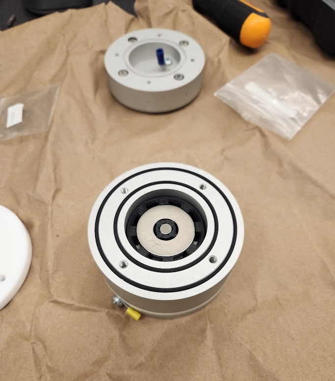
The sputter head was the key feature added to the chamber for V1 and is used to secure the target and create & contain the plasma used to sputter the target onto the silicon substrait. The sputter head’s internal components are at atmospheric pressure and are sealed from from the surrounding, near zero pressure. This was done to allow for the electrical and cooling to connect to reach the internals of the sputter head without requiring expensive passthroughs.
Future iterations will focus on removing the welding when connecting the sputter head to the lid of the chamber due to the lid warp ing under the heat of the welder. This will improve the plasma generated by the chamber, improve sputtering rates, and be easier for people to make the chamber for themselves.